| |
|
|
A to D CONVERTERDESCRIPTIONThis product is obsolescent and should not be used for new designs with a long lifetime. The TDS9096 is an eight input analog to digital converter with �5V input range and resolution 12 bits plus sign. Software file _TDS9096.TDS is provided which allows conversion times of 114�s (any channel at random) or 140�s (continuous single channel). The output is -4096 to +4095 as a 16-bit two's complement number, each unit of output corresponding to about 1.2mV input. When using TDS9096 with the TDS9092 or TDS2020F, no features of the computer are lost. For example, all the I/O lines (and 10-bit 8-channel A to D in the case of the TDS2020F) are still available. The TDS9096-PIN and TDS9092-PIN (or TDS2020F) sandwich to make a small module, or you can use the -PLUG versions in a rack.
PROCESSOR INTERFACEThe TDS9092 provides the data bus and control signals to the TDS9096. The board can be placed in one of three positions in the address map, selected by the position of a jumper link on the TDS9096:
018C-018F 019C-019F 01AC-01AF
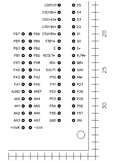
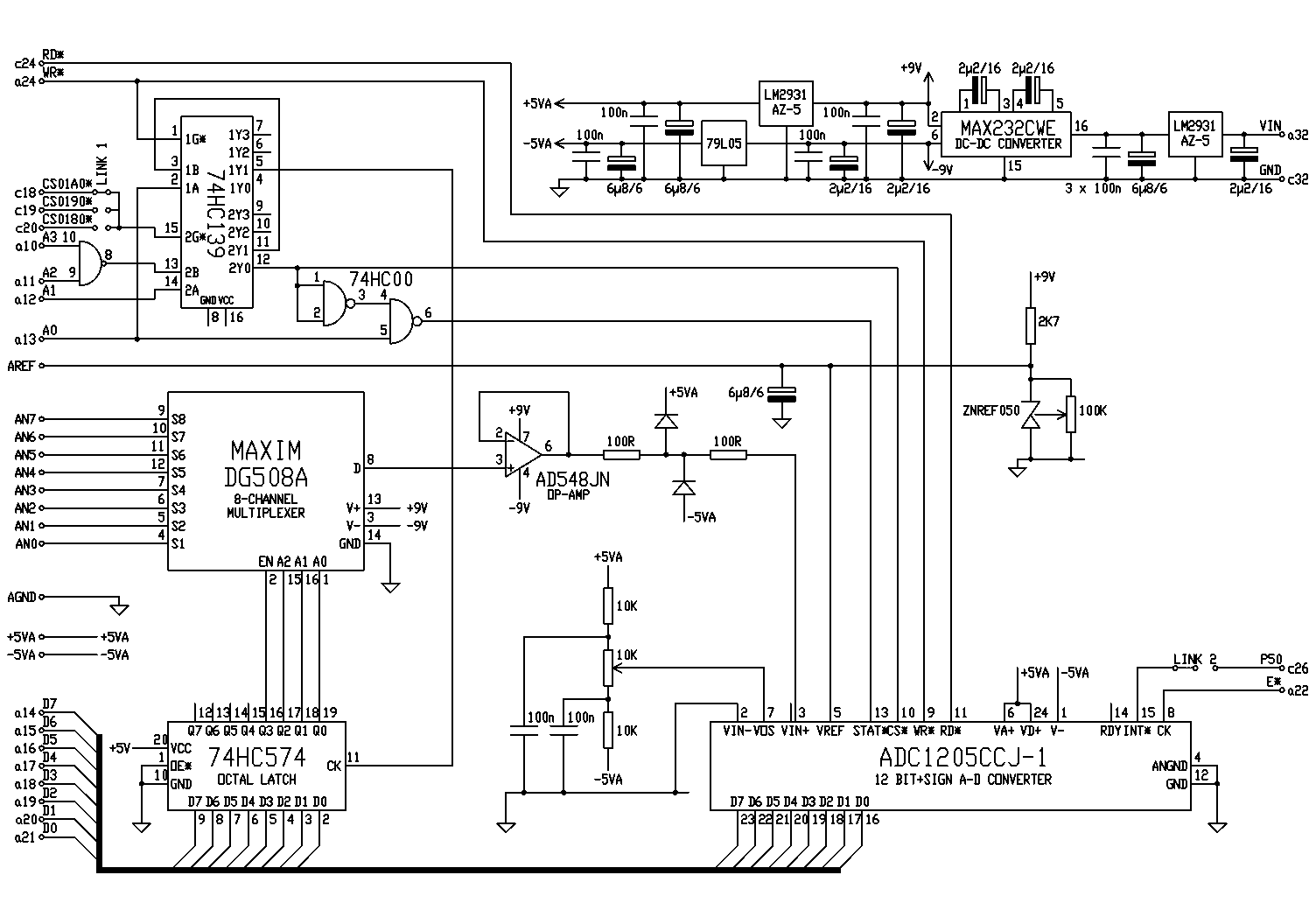
On delivery, and in the software provided, the last of these options is selected. Make sure that no other peripherals are added in the same address space. If more than one A to D converter is used with one computer, select a different address for each. ANALOG MULTIPLEXERA low power version of the DG508A multiplexer selects one of 8 input channels. The input range is �5V on each for full conversion range and up to �9V can be applied without damage. The choice of channel is made by writing to address 01xF where x is 8, 9 or A as selected by shorting link. Bits 0 to 2 choose the channel number 0 to 7 while bit 3 enables the multiplexer at logic 1. An AD548 CMOS op-amp buffers the output from the DG508A. It has a slew rate of 6�s between extremes of input range. A TO D CONVERTERThe conversion is performed by a CMOS ADC1205 device. Its input is protected from over-voltages of up to �9V by clipping diodes. Multiturn potentiometers OFFSET and GAIN are used to adjust for zero and range respectively. These are set on manufacture but should be checked and trimmed if necessary. The output is read from address 01xC where x is 8, 9 or A. The address is read twice, the first byte is the upper, and the second the lower one. The sign bit 12 is repeated in bits 13 to 15 which ensures that when the two bytes are put together a twos complement conversion is directly obtained. For further details see the ADC1205 data sheet from National Semiconductor Inc. Provision has been made for the interrupt output of the chip to be routed to IRQ1* on the TDS9092 computer by means of a shorting link, however polling of the device in software provides a fast conversion stream without interrupt handling. REFERENCE VOLTAGEThe reference voltage is stable to typically 0.1mV over for a change of power supply from +6 to +16V. It is adjusted by the GAIN trimmer. POWER SUPPLYThe single wide-range input voltage +6 to +16V is regulated to +5V by a low voltage drop-out device. A DC-DC converter then provides �9V which in turn is regulated to give +5V and -5V. These rails are substantially isolated from changes in the supply to the board. This, and the 30mA current, allow battery operation if required. The final +5V and -5V supplies are brought out on pins +5VA and -5VA to power any input signal conditioning needed by the application. The reference +5V is also available between AREF and AGND. PHYSICALThe size is 100 x 72mm and there are four corner mounting holes for 2.5mm screws. The TDS9092's connections and hole positions match each other. The diagram of a corner of the TDS9096 shows the position of the extra pins: the 8 analog inputs AN0 to AN7, �5V output, voltage reference output and ground.
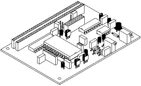
There are two versions, which differ only in the 64-pin connector. The TDS9096-PLUG has a DIN41612 type C plug and is suitable for rack mounting (it is a short Eurocard). The TDS9096-PIN can be sandwiched with the TDS9092-PIN computer to form a neat module with all the computer pins repeated on the underside of the A to D board so that nothing is lost. Alternatively mount the computer and TDS9096-PIN alongside each other on a motherboard, for instance on a 160 x 100mm eurocard. We stock suitable motherboard sockets under the order code PINSOCKETSET.
TDS9096 circuit diagram |
 |