| |
|
|
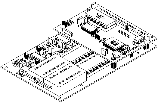
TDS961 PROM PROGRAMMER BOARDOVERVIEWThis product is obsolescent and should not be used for new designs with a long lifetime. One way to make a PROM at the end of development is to switch off, take the non-volatile RAM to your programmer and copy it into PROM but there is another more direct way. The TDS961-PIN is a Eurocard with pin sockets designed to take the TDS9092-PIN computer. The pair go together as a sandwich. Using software supplied, the developed program is transferred into PROM. The TDS961/TDS9092 combination can also be used as a general purpose programmer. All types from 2716 to 27256 (16K to 256K bits) are handled, including 21V programming ones. There are two 28-pin programming positions. A rack version with DIN connector is also available.
Both are Eurocard size (160 x 100mm). The TDS961-PLUG has a DIN41612 type C connector for use in a rack; TDS961-PIN which is identical except for the connector. This has a 64-way straight socket into which you can plug a TDS9092-PIN computer directly. The socket is extended on the other side of the board with wire-wrap pins so that access to all connections is still available. The boards have two 28-pin zero insertion force (ZIF) sockets for programming one or two PROMs at once. Types programmed are the following:
2716 2732 2732A 2764 27C64 27128 27C128 27256 27C256
Software supplied indicates continuously the status of programming. For example it shows the check for correct erasure, programming done in percent, and the final verify. A quick programming algorithm is used. INSTALLATIONTDS961 boards are used in conjunction with any of Triangle's Forth instrumentation computers but this documentation mainly refers to the TDS9092. Backplane pin connections are identical and the TDS961 board can be strapped in parallel with the computer. A particularly suitable combination is the TDS961-PIN and TDS9092-PIN which together form a stand-alone PROM programmer, as well as TDS9092 development module. The only essential connections to the TDS9092/TDS961 pair are these:
The programmer draws all its power requirements from the pin a32, which should be a laboratory supply of +12V capable of at least 1A peak current. The circuitry on the board converts this to +25V, +21V, +12V and +5V required by PROMs. There are potentiometers for fixing these voltages. They are pre-set at manufacture and should not need further adjustment. The programmer sits at this address:
The address is determined by which of 3 links is made on the board. On delivery the address is 0190 and the software provided assumes this. It is readily edited to one of the other addresses if required. The boards come complete with PROM programming software. This is supplied in two forms:
q Forth source code program _PROM.TDS supplied with TDS-PC development software for TDS9092 q Turnkey PROM with the same program. This can be inserted into the TDS9092 to give an instant stand-alone PROM programmer.
The software is in two parts and a comment separates them. The first part is essential PROM programming software. It occupies about 2K bytes when compiled. The second part is optional. It provides the user with an easier interface and on-line help. Both parts are in the turnkey PROM and we suggest you use both until familiar with the programmer. The second part could then be dispensed with. The software descriptions below assume use of both parts. Installation of the software depends on what you are doing:
q To use the PROM just plug it into the TDS9092, change the links for 32K PROM use (see PCB LINKS) and power up. This gives a stand-alone PROM programmer for reading, editing and copying PROMs. q To compile the program into RAM on the TDS9092 follow your normal procedure for Forth program compilation. For example just press F8 if using a PC and respond with the filename _PROM.TDS
To blow an application program into a 27C256 PROM follow this sequence:
1. Turn on the TDS9092/TDS961 combination 2. Compile the application program, ending it with SET WORK or any other method of setting the cold-start parameters 3. Type HERE HEX U. and note the address the dictionary reaches up to 4. Compile the file _PROM.TDS from the TDS-PC disk 5. Type WORK to start off the PROM programming software 6.
Set PROM type with PA27C256 LOWER . Put the PROM into the
lower socket with the notch nearest the board edge and then program with something
like:
See also PROGRAMMING PROMS. PIN CONNECTIONS
Names and pin connections are those for the TDS9092 and other computers. INITIALISATIONType WORK to initialise the software compiled from file _PROM.TDS. The set-up sequence leaves the computer in hex. To access on-line help at any time just type HELP return. This gives you a menu of several pages of assistance. On power-up the PROM type 27C128 and 12V programming is set and the LOWER programming socket is selected. To choose one of the others type the name preceded by P and then the socket(s) required. Never change device kind with a PROM in a programming socket. Examples:
Note that the large 27C256 PROMs are treated as two individual PROMs. Socket selection after the PROM type is essential since the name de-selects both sockets. If the PROM is 2764 or larger and needs 21V programming, then add 21V after selection like this:
P2764 BOTH 21V
Every time you program you will now be asked to confirm the 21V by responding 21 or 12. This is to help avoid any damage to 12V programming types. It is not always clear from the package which type the device is. Consult the data sheet or try 12V first. At any time you can revert to 12V programming by typing 12V . PROGRAMMING PROMSAfter setting up the system as previously described put the PROM(s) to be programmed into the board (if only 24-lead then leave holes l, 2, 27, 28 free). Then use the word PROGRAM as in the following example to write to the device. Note that two PROMs can be programmed in parallel with identical data if BOTH was selected.
4000 5000 0 PROGRAM ( example of programming
The three numbers are
q first address containing data to go into the PROM q address after the end of the data q address in the PROM at which programming is to start.
Note that only part of a PROM can be programmed if required. The example above programs memory addresses 4000 to 4FFF inclusive to addresses 0 to FFF in the PROM. The word PROGRAM shown above also verifies the data written. If the device is not programmed correctly (e.g. bad PROM, incorrectly inserted, etc.) then the terminal will beep once and a message appears. If successfully programmed the terminal responds with a double beep and the Forth system returns ok . The verify is done after every byte, and also a global verify is made at the end of programming. A fast programming algorithm is used but times depend on manufacturer and data being programmed. Be prepared for several minutes wait. As programming progresses the percentage complete appears continuously on the screen. READING PROMSEnsure the system has been set up as described, including initialisation by P27C128 UPPER or something similar. To read a PROM put the device in the appropriate socket and use the word READ as in the following example:
100 200 6000 READ ( example of reading 6000 100 DUMP ( look at the data
This would read PROM addresses from 100 up to, but not including, 200 to address 6000 in memory. An automatic verify is done after reading. VERIFYING PROMSTo verify that a given PROM contains the same data as a given area of memory use VERIFY after the set up command. For example:
1000 1800 6000 VERIFY ( example of verification
This would check that PROM locations 1000 up to but not including 1800 are the same as data in memory from address 6000 onwards. COMPARING TWO PROMSTo check one PROM against another the commands can be combined in the usual Forth way. For example use P27C128 then:
: COMPARE27C128 ( example of PROM comparison UPPER 0 4000 9000 READ LOWER 0 4000 9000 VERIFY ;
COMPARE27C128 checks that a 27C128 in the upper socket is the same as a 27C128 in the lower socket. COPYING PROMSThis is a combination of READ and PROGRAM . For example for single copies of 27C64 PROMs the following word can be defined:
: TRANSFER ( example of PROM copying UPPER 0 2000 6000 READ ( upper device to memory LOWER 0 6000 8000 0 PROGRAM ; ( program lower one
To make many copies read the master to memory then program using both sockets. SOFTWARE EXTENSIONSThe TDS961 software can be easily extended to include other features useful in particular cases such as device serialisation, reading a PROM and sending the data to the serial port, and so on. The normal Forth system is available for all such functions, and use can be made of all the more primitive programming words which are defined in the software supplied with the programmer board.
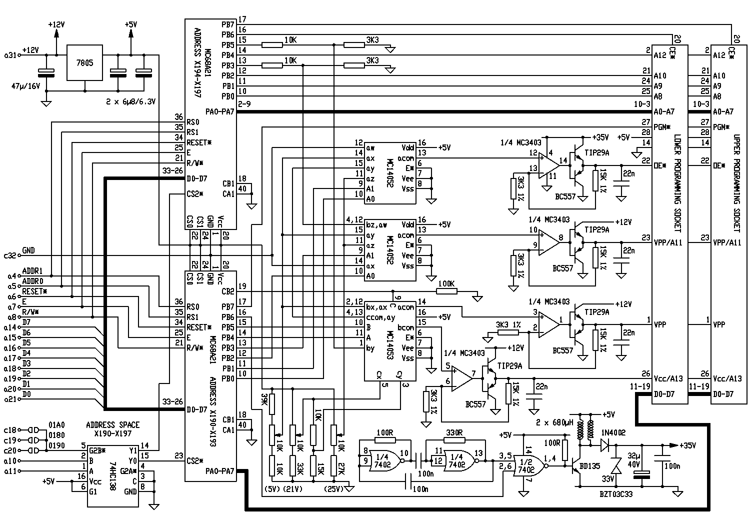
TDS961 circuit diagram |
 |