| |
|
|
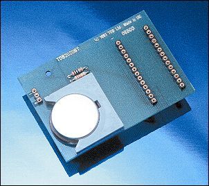
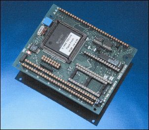
TDS2020F SPECIFICATIONSCONTROL COMPUTER & DATA COLLECTION MODULEOVERVIEWThe TDS2020F is a powerful 16-bit control computer. Despite the small size and low power consumption, it is packed with important features that make it easy to use in solving control and data collection problems. Rapid application development is assured by the interactive nature of development and debugging. A library of software provides instant solutions to many application problems. Source code, written in the high level language Forth, is directly compiled into Flash-EEPROM non-volatile memory. Coupled with the ready-made software modules, designs can be completed very quickly, even without a prior knowledge of Forth. WHY FLASH?Direct compilation to Flash-EEPROM is convenient and avoids the cost and development cycle of a PROM programmer. There is a further advantage-you can zap the program remotely over a modem and recompile. Suppose the TDS2020F were embedded in a vehicle or a pressurised vessel, you could update the program without even removing the computer. WHY FORTH?The reason for programming card computers in Forth is productivity-you get results faster with less cost. It is closer to the machine than 'C' but is a higher-level language than assembler. Unlike either, it is interactive, giving quicker development. The multitasking Forth specially written for the board gives easy access to all its features and allows software to be written quickly. It is American National Standard Forth with many extensions to exploit the hardware features of TDS2020F. The 16k-byte Forth includes LCD and keypad drivers, together with many other utilities and a full symbolic assembler. You write programs in high-level language, mixing it with assembler if required. WHAT HARDWARE?The TDS2020F is based on the Hitachi H8/532 microprocessor. There are 45k bytes of space for your compiled program and up to 512k bytes of Flash memory or battery-backed RAM to keep vital data while the board is not working. This can be expanded to over a gigabyte with plug-in PCMCIA or Compact Flash cards. A Controller Area Network adapter (CAN bus) allows fast interconnection of TDS2020F computers, with a PC in the network if required. Both low level and high level widely used CAN protocols are provided. The board has between 26 and 41 Parallel I/Os depending on the other options selected and there are two RS232 Serial Ports. The Analog to Digital converter has eight channels of 10-bit resolution (better than 1 in 1000) and there are three channels of 8-bit Digital to Analog (1 in 250). Additional features include four hardware Counter-Timers (three are 16-bit), two separate Watchdog Timers, non-volatile Time-of-day Clock and Multitasking. The single power supply draws 32mA with only 155�A in a low power operational mode for applications like datalogging. The TDS2020F measures just 100 x 80mm, it has pin headers for connection by ribbon cable; or simply use it as a component inserted on a larger board. Another version has a DIN41612 connector for use in a rack. USING FORTH IN THE FIELDWhen you finally reach the manufacturing stage with a TDS2020F based product it is not the end of Forth. Use it for final test, repair and maintenance because the language is on-board. Build in a connector that gives serial access to the Forth computer in your instrument. Now, with a PC or hand-held terminal, gain access to the internal language system. You can have available all the functions which make up the application. For example, in an electronic thermometer the Analog to Digital routine can be separately exercised to see if the fault is in the in�put transducer or amplifier. If not, follow with a test of the LCD by writing a few char�acters to it. Likewise, test the keypad by pressing a key to see if it returns the expected code. If necessary, the whole of the compiled code can be erased from the Flash-EEPROM. New source-code can then be recompiled, even remotely over a modem (or into an inaccessible location). No chip or link change is needed to make a stand-alone system. On-board Forth is very useful during design, but the ability to ac�cess an individual software procedure in a finished product is unique and invaluable. SPEEDThe TDS2020F clock frequency is 19.6608MHz and the microcycle time 102ns. Instructions are processed at an average of around 3 million per second (MIPS). Another measure gives 1600 dhrystones/second. The interrupt latency time is only 2.3�s, plus the time to complete the current instruction. MEMORYInside H8/532: 32k-byte one-time programmable PROM carrying 16k Forth high level language and 16k blank space for additional user application program. A TDS2020DV development piggyback board is available to emulate this memory but is not usually needed.
TDS2020DV Inside H8/532: 1k-byte RAM, of which half is needed for the system leaving 512 bytes free for use as variables by the application program. Many control uses will need no further RAM memory. 28-pin socket: 32k-byte non-volatile Flash-EEPROM for the final user application program. Because some of this part of the memory map is used for I/O and on-chip registers only 29k bytes are actually available. The TDS2020F is priced with this socket empty, although the TDS2020F-SP Starter Pack includes a 32k-byte static RAM and Flash-EEPROM for this position. Once the software is finalised, the socket can hold a 27C256 EPROM if desired. 32-pin socket: 512k, 128k or 32k RAM, EEPROM or Flash memory for additional variables, scratchpad arrays or data storage. EEPROM and Flash keep data with power off; the RAM can be made non-volatile by adding the TDS2020BYN (piggyback) or TDS2020BYD (separate) battery board or an external lithium cell. Circuitry to ensure that data will not be corrupted is built into the TDS2020F. Signals are available to indefinitely expand the memory off the board. The TDS2020F is priced with this socket empty. Clock chip: The on-board clock chip has 239 bytes of free RAM that are accessible over the I2C bus. If the TDS2020BYN, TDS2020BYD or other battery is added, this RAM (as well as the real-time clock and any RAM in the 32-pin socket) will be retained while power is off.
TDS2020BYN PARALLEL INPUT-OUTPUTThe parallel port capability of TDS2020F depends on whether the analog and other facilities are used or not. The table shows only some of the I/O plans that are possible:
Pins can be set for different functions so the number of free parallel inputs and outputs depends on whether Analog to Digital conversion, non-volatile Time-of-Day clock etc. are needed. From this table you can check how many spare ports are available. In summary, the number of parallel input or output bits is between 26 and 41 depending on other facilities used. The number is easily expandable. I2C BUSThis is a two wire system for use with low cost peripherals such as A-D converters, clocks, I/O, RAMs, EEPROMs etc marketed by Philips, Signetics, Xicor, Microchip Technology and others. The board has a PCF8583 clock chip and RAM connected on this bus. Other I2C chips can be added externally. SERIAL INPUT-OUTPUTOn the board are two serial drivers and receivers using true RS232 format and voltages. They can be used to give a single asynchronous serial link with handshake or as two separate serial links without. All baud rates 75 to 38.4k are supported on Port 1 and there is the additional MIDI 31.25k baud. Port 2 can be used at all rates up to 4800 baud. Although the computer has a single power supply of +6 to +16V, the serial ports use �8V generated on board to give output logic levels that meet RS232 specifications. MICROPROCESSORThe microprocessor is H8/532, a 16-bit device with eight general-purpose 16-bit registers, hardware 16-bit multiply & divide and 8 & 16 bit instructions. Direct bit manipulations operate with registers, all memory and input-output. The crystal frequency is 19.6608MHz and the device runs in the expanded maximum mode with a 1024k-byte memory space. It has much on-chip hardware including three 16-bit counters or timers, one 8-bit counter/timer, synchronous or asynchronous serial port and a very versatile interrupt system (65 interrupts and DTC vectors, 8 priority levels). The Data Transfer Controller (DTC) enables transfers between I/O and memory without any software. All the capabilities of the processor are available to the TDS2020F user, but through the high level language Forth, which makes them easier to employ. Access to some of the microprocessor hardware facilities is already built into the Forth system but the user is free to use them in his own independent way, via Forth or assembler. See the TDS2020HM Hardware Manual for full details of the microprocessor. KEYPAD SUPPORTA unique software and hardware system enables up to 64 keys to be connected to the computer and only eight of the parallel input/output lines are required. You connect a particular parallel output port to one side of an 8 x 8 key matrix via diodes. The other side is returned via another eight diodes to the data bus. The Forth system has words that scan the keypad and return 0 if no key is pressed and 1 to 64 otherwise. LIQUID CRYSTAL DISPLAYSAny alphanumeric LCD based on the HD44780 chip connects directly to TDS2020F; software to drive it is built into the card. One external chip enables up to eight LCDs to be connected and the software caters for them all simultaneously. Graphics LCDs also connect without any extra hardware; driver software is supplied on disk for displays based on the HD61830, T6963C and other graphics controllers. Examples are:
LMG6401PLGE (Hitachi)
MGLS12864TLV2CCFL (Varitronix)
With extra hardware incorporating a controller chip, �-VGA to full VGA displays can be attached to TDS2020F. EXTERNAL PERIPHERALSThe full data and address buses as well as five uncommitted decoded addresses for use as chip selects of peripherals are provided. LCDs, extra parallel I/O, a quad serial port chip or similar devices can be added without any interface chip. Each decode covers a memory span of 16 locations. Three are not strobed with the E clock signal and are suitable for driving most peripherals such as octal latches or graphics LCDs. The other two are strobed with E. One is negative active, the other positive active. The latter is exactly right for input to alphanumeric LCD displays. ANALOG TO DIGITAL CONVERTERThe TDS2020F has an eight channel 10-bit A to D converter giving one part in 1024 resolution. Conversion time is 21�s using a supplied library program although a 127�s Forth version is built into the TDS2020F as standard. An input voltage of 0V gives 0 and +5V gives 1023. The on-board reference is 5.00�0.05V and there is facility for connection of an external reference. If the A to D is not used, the eight pins automatically become extra parallel input ports. DIGITAL TO ANALOG CONVERTERThere are three channels of 8-bit Pulse Width Modulated (PWM) D to A conversion that act as three extra bits of parallel I/O when not used. For example, you could choose to output a 20kHz waveform with a mark to space ratio of 40:210. Add an external filter (such as a 10k resistor and 1�0 capacitor) to get the analog level, 5.00V x 40/250 = 0.8V in this case. NON-VOLATILE TIME & DATETDS2020F has a PCF8583 clock chip that keeps date and time even with the computer switched off provided a TDS2020BYN, TDS2020BYD or external battery is added. The battery is also used to maintain up to 512k bytes on-board static RAM. A typical consumption is 3.5�A, giving the battery board a lifetime limited by the 5 year shelf life rather than the 950mA-Hr capacity. Date & time are accessible to a resolution of 813 nanoseconds because another clock running under interrupt mirrors the chip clock. Both European and USA date formats are supported. The clock chip generates a one-second Non Maskable Interrupt (NMI). This does nothing by default, but it can be redirected to execute a user routine in either high-level Forth or Assembler. The repeat time can be changed in very small steps to give intervals from 30ms to a year. TIMER-COUNTERSThere are four hardware timers (plus the clock chip); one is 8-bit and the other three 16-bit. Each can be clocked internally at any of three rates, or externally for event counting. They all have two output capture registers and the three 16-bit timers have an input capture mode. Multiple interrupts are associated with the timers to process asynchronous events in high level Forth or assembler. WATCHDOG TIMERSIf the microprocessor crashes through a power spike or otherwise, one of the watchdog timers will reset the system. The application program will be started again. There is an internal watchdog (default 106ms) and a counter external to the microprocessor (426ms). Both are reset by many Forth words and normally you will not notice their action, but will time out and restart the system if something goes wrong. On restart, you can either enter a user-defined Forth word or accept the default warm reset. LOW POWER MODEYou can switch off power to the RS232 driver and put the microprocessor into software standby mode. Current consumption is now down to typically 155uA plus any external loads. When a Non-Masked Interrupt occurs the computer will wake up, turn on the serial port and continue program execution. This makes the TDS2020F ideal for portable and data collection applications. POWER SUPPLYA single supply of +6V to 16V is used, typical current 32mA. A low power operational mode consumes only 155�A and needs no external hardware support. The board has a �8V generator for use by the serial ports and this can be turned off by software to save power. The negative supply is also useful for some external peripherals. The regulator on the board can supply up to 100mA so there is extra current available to power any external circuitry particular to the application. BUS INTERFACEThe TDS2020F bus is compatible with almost any peripheral chip such as A-D converters and multiple serial port devices. The data bus is not multiplexed. In practice, limit the length of the data and address buses off the board to 300mm unless you extend it with the suggested circuitry. PHYSICAL
The board size is 100mm x 80mm with mounting holes for 2.5mm screws. Maximum height, excluding pin connectors, is 15mm. With the TDS2020F in pin sockets of the type stocked, the distance between the computer and the motherboard is 11�1mm. This should be the length of spacers, if used. The operating temperature is -10 to +70�C (-20 to +75�C or -40 to +85�C to special order). Pin connectors are standard (TDS2020F) with a DIN 41612 type C connector optional (TDS2020F-PLUG). The connections all fall on a 0.1-inch matrix so that the board can easily mount on a prototyping board with a matrix of holes if required. There is a blue reset button in the corner of the board. ANS FORTH SYSTEMThe language is a full implementation of American National Standard Forth including floating point and contains:
q All CORE word set q All CORE EXTENSION word set q All DOUBLE NUMBER word set q All DOUBLE NUMBER EXTENSION word set q All EXCEPTION word set q All STRING word set q All FLOATING POINT word set (extra charge) q
From the FACILITY word set these words: q
From the PROGRAMMING TOOLS word set these words: q
From the SEARCH ORDER word set these words:
There are many extensions useful to developers of single board systems. For example, the number of microseconds taken by any Forth word can be accurately measured in real time. The language has been specifically implemented for the H8/532 microprocessor. It uses the chip's facilities wherever possible, e.g. Forth multiplies and divides are built up from the 16-bit hardware multiply/divide instructions. Its bit manipulation instructions are also employed, they are especially useful for detecting and switching single I/O lines. All Forth registers are implemented in microprocessor registers and the parameter stack is the same as the machine's hardware stack. The two Forth stacks and user variables are all in the memory inside the microprocessor chip for maximum speed of access. Two machine registers are (usually) left free so that they can be used by fast interrupts without the need to store them. The application code is compiled into non-volatile Flash-EEPROM to instantly create a stand-alone system. Apart from Forth, the system ROM has a symbolic assembler enabling you to write machine code directly on the board. No cross-assembler is necessary so an assembler routine can be tested immediately without needing to download a binary file. Interactive debugging of assembler code is very powerful. The ANS Forth system is copyright Triangle Digital Support Ltd and purchase of a TDS2020F or chip set conveys a licence to make one copy. There are no royalties of any kind, even though the Forth can be left available for your customer to use. FORTH ROM EXTENSIONSAmong the extensions included in the Forth ROM are:
q Keypad scanning q Alphanumeric Liquid Crystal Displays q I2C bus peripheral support including on-board clock & RAM q Interrupts written in assembly code or Forth q Multitasking q Time of day clock q Watchdog timer servicing q Low-power operation q Complete symbolic assembler q Vectored serial I/O and several other vectored words q Hex, ASCII & control characters in forms $A4FF "A ^A q Double number (32-bit) arithmetic and stack handling e.g. M* 2ROT q Execution time measurement accurate to 1�s MULTITASKINGDevelop printer, display and communications programs as separate entities, then using the pre-emptive multitasker let them run all at once on the TDS2020F. Debugging of each task can be done independently of the others using the interactive Forth facilities that allow running of a sub-program just by typing its name. The final stage is to combine the individual programs, essentially a mechanical step following rules. Perhaps the most important use is to make the interactive Forth language one of the tasks. This adds an exciting new dimension to debugging embedded systems. For example in an electric vehicle you could monitor and adjust performance while in motion via common variables. While you type in new commands, other tasks will continue controlling motors, displaying results on a graphics LCD and collecting performance data on a Compact Flash card. INSTANT SOLUTIONSSoftware modules that easily connect can form the major part of your application program. Ready-made routines are available for the following. For more details see the Applications Software datasheet. Most are free on the Starter Pack CD but extended multitasking and other utilities are available through the Update Service. In addition, for a fee there is a fully featured floating point package for the TDS2020F, order code TDS-FLOAT-ANS.
DEVELOPMENT REQUIREMENTSThe development environment TDS-PC for Windows is PC software with terminal emulation and multiple-window editing facilities. Source code is stored on the PC disk, although compilation takes place inside the TDS2020F. One key starts the automatic process that sends your source program from the PC's serial port to the TDS2020F for compilation there. The code is then debugged interactively in the TDS2020F. TDS-PC for Windows also runs on Macintosh PC emulators. Source code can be laid out with lots of comments and correctly indented structures. Single keys invoke compilation and other features. There is an INCLUDE facility so that source files can be nested. There is interfacing to your usual source-code text editor so that writing is made easier. Once your program is developed and working nothing else is needed for the standard development arrangement. No PROM programmer is needed because the code has been compiled into non-volatile Flash-EEPROM. PCMCIA & COMPACT FLASH DATA LOGGINGThe TDS2020CM2 sits on top of a TDS2020F board to form a data logger module complete with ejector mechanism. PCMCIA memory cards (PC cards) and hard drives can be used. See DATA LOGGING TO COMPACT FLASH AND PCMCIA, page 250. Data is recovered from a PC card through a PCMCIA drive for your PC. Notebooks have them in-built but internal and external models are available for desktops. The PC card is formatted for Windows. Comma separated variable format is a good way to write the data in the TDS2020F so that the PC can read the data directly into an Excel spreadsheet or Access database. Compact Flash cards as used in digital cameras can also fit into the TDS2020CM2. You need to remove the ejector by unfastening two screws and to add the TDS2020CFA Compact Flash converter to change the 68 pins to 50 pins. One advantage of Compact Flash is that the edge of the card is flush with the edge of the TDS2020F making it easier to mount the module in a sealed box. NETWORKINGController Area Network (CAN bus) sends messages of up to eight bytes. Each of these frames has an identifier and any node with a matching identifier will receive the message. The bus is the basis of CAL, CANopen, DeviceNet, P-CAL, SDS, CAN Kingdom, and the network used by the automotive industry in cars and trucks. For full details, see CONTROLLER AREA NETWORK (CAN BUS), page 282. Each node can be a TDS2020F+TDS2020CAN or TDS9092+TDS2020CAN combination, or a PC. The network may have up to 110 daisy-chained nodes with a total network length up to 1000m. It typically uses two twisted pairs, one for signal, one for power. BACKWARD COMPATIBILITYPROM programmers are outdated in many applications. The Flash Forth kernel has direct compilation to a Flash-EEPROM non-volatile memory chip. It is not necessary to blow an EPROM any more. The last hurdle in developing with TDS2020 has been eliminated. The new version 4 kernel is an update of ANS Forth version 3.07 and 3.07A. This Flash Forth is the version for new developments. It is not binary compatible with earlier versions-applications should be recompiled. See UPGRADING AN OLDER TDS2020, page 236. TDS2020F FORTH CHIPSAs well as forming the basis of the TDS2020F computer, the microprocessor, gate array and software are also available as a chip set for use in other embedded systems. See FORTH CHIPS, page 336. TDS9092 EMBEDDED COMPUTER
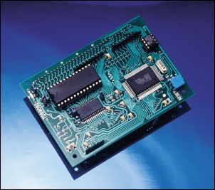
TDS9092-PIN card computer This is the TDS2020F's smaller brother, not quite as powerful but cheaper. Ask for the datasheet. Especially low prices can be quoted for TDS9092 in quantity. Any A to D or D to A requirement must be added externally as additional chips. However, it still interfaces with LCD and keypad, has two serial ports and drives I2C peripherals. Its pin connections are virtually identical to the TDS2020F and the Forth can easily be converted. You can readily migrate between the two. Conversion of a TDS9092 application to TDS2020F should be straightforward. The size of TDS2020F is larger at 100 x 80mm (against 100 x 72mm) but the four mounting hole and reset button positions are unchanged. As far as possible, TDS2020F pin connections correspond to equivalent ones on TDS9092. There is an extra row of 32 pins named z1 to z32 and the internal connectors are not there, except for ports A and B. Most pins correspond to those on TDS9092, but some names change to match the H8/532 Hitachi documentation. The actions of Forth words with identical names are mostly the same on both TDS9092 and TDS2020F. Programs may need only small modifications to move them from one to the other. ON THE WEBLatest support software for TDS2020F is available on the Web at www.TriangleDigital.com. Both the TDS-PC for Windows development environment and ready-made software modules can be downloaded. Apart from files reserved for Update Service customers, most software is free of charge. The Web pages also contain the text of principal data sheets. There is a summary of each library routine, readily accessible from an index. The site includes details of many TDS2020F applications and links to the pages of some customers. PRICES AND E-COMMERCEProduction ceased September 2008 following an announcement over three years earlier in May 2005. The web shop is now closed. To satisfy essential repair requirements, small quantites, sometimes on extended lead times, are available. . |
 |
|