| |
|
|
PARALLEL INPUT & OUTPUT EXPANSIONOVERVIEWTo achieve I/O expansion you can use the serial two-wire I2C bus and I/O chips or hang octal parallel integrated circuits on the data bus. These are discussed in turn. See PARALLEL INPUT & OUTPUT, page 74, for more details of I/O. I/O EXPANSION ON I2C BUS
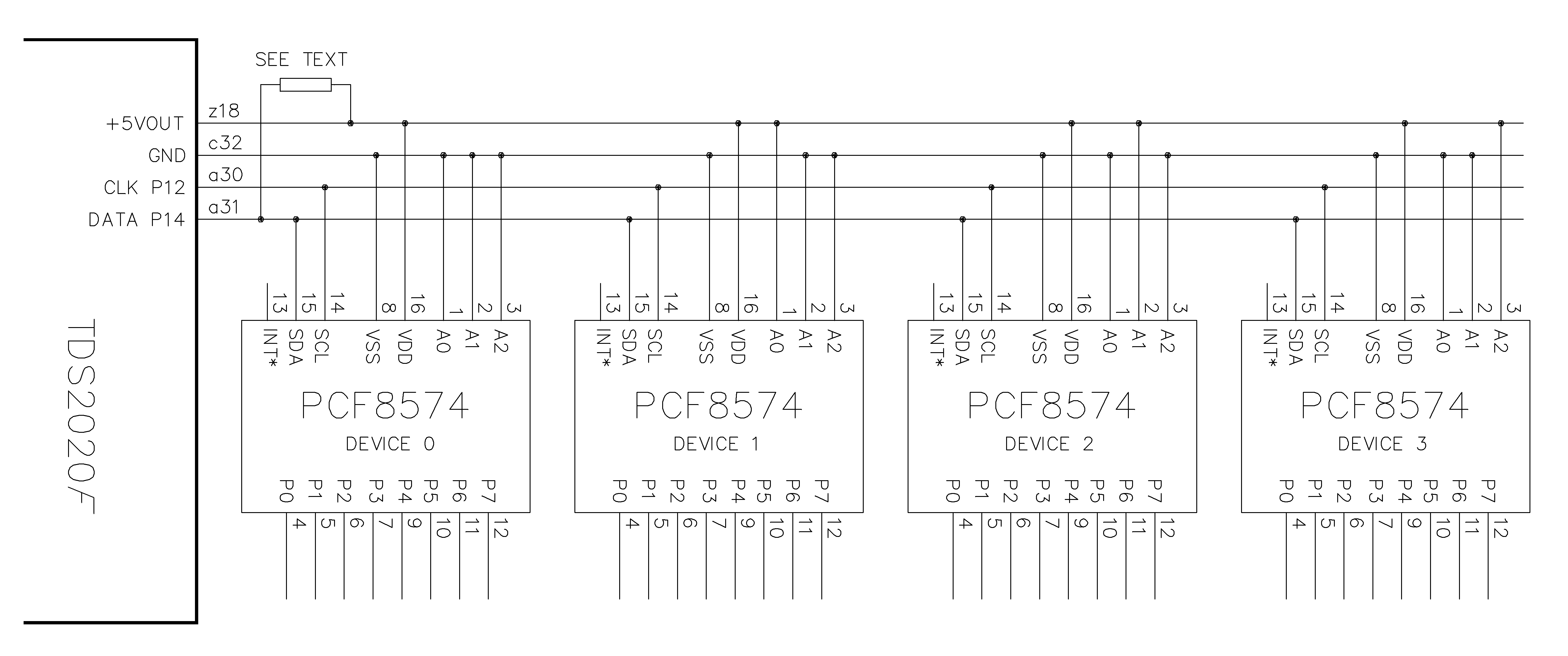
I2C expansion The PCF8574 & PCF8574A from Philips offer 8 bits of parallel input or output. These low-cost chips are very useful for expansion, particularly since you can connect up to 16 devices, giving 128 I/O lines, to just 2 wires of the I2C bus from the TDS2020F. They can be a few metres from the computer board. Because of capacitive loading on the I2C data bus the 100k internal pull-up on the TDS2020F may be too high. Check with an oscilloscope on pin a31 and ensure that the signal rises to logic 1 within one bit time of the waveform. If not, add an external resistor from Port 1 bit 4 (pin a31) to +5VOUT (pin z18). Try 100k then lower, the value needed will depend on how many I2C chips are connected, how long the wires are and whether the TDS2020DV piggy-back board is used or not (it is slower). The file #PCF8574.TDS (comes with the Update Service) has the software support. To use an I/O as input, first write hex FF to it (only needs to be done once). For example:
$66 7 !8574 \ output 8 bits to PCF8574 \ device number 7 $FF 3 !8574 3 @8574 \ input 8 bits from PCF8574 \ device number 3
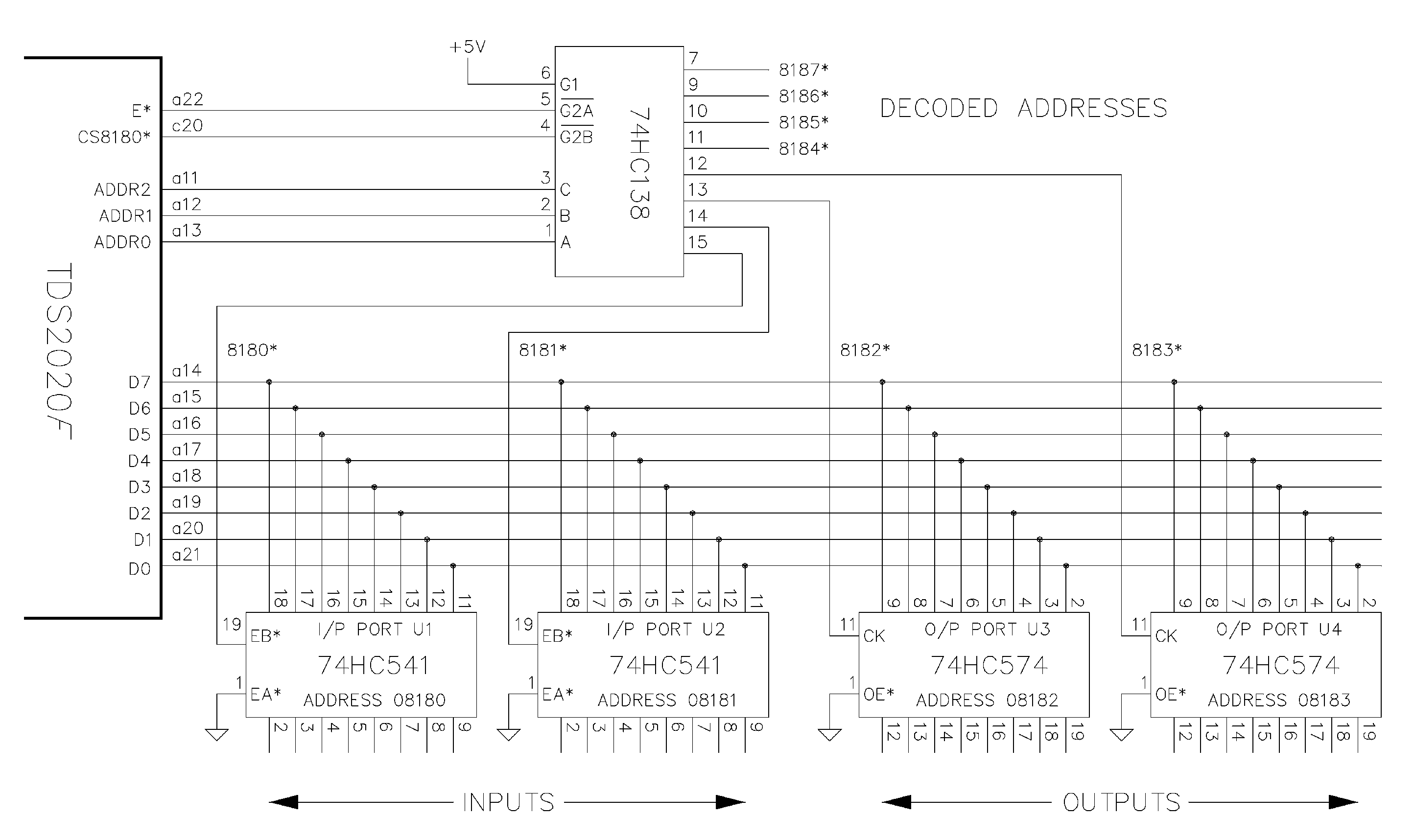
Each IC has 3 pins, which you tie to 0V or +5V to code for the device number. Note that the TDS2020CM2 PCMCIA adapter (if present) uses addresses 6 & 7 of a PCF8574A. I/O EXPANSION ON DATA BUSFor an 8-bit output use an octal latch type 74HC574 and for an input an octal buffer 74HC541. You need negative active address decode lines for these such as the spare chip selects provided on the TDS2020F connector, splitting them further with another decoder if you wish (see diagram).
I/O expansion on the data bus The basic Forth word to output the top of the stack to such a parallel 8-bit port is PC! and to input 8 bits from 8 logic inputs to the top of the stack is PC@ . For example $1F $8182 PC! puts the binary pattern 00011111 to address 08182 so that it will appear at the output of the third chip from the left in the diagram. The three pins 12-14 will go to 0V and the five pins 15-19 will be +5V. To work with individual bits use the logic operators OR AND XOR INVERT . Note that an output port implemented as shown can not be read back so in cases where individual bits are being manipulated a copy should be kept in RAM. For example, to output a pulse of 1ms on bit 3 of the chip on the right (i.e. address 08183):
VARIABLE 1MEMORY \ For O/P port copy : INIT ( - ) \ Part of switch on initialisation 0 1MEMORY C! 0 $8183 PC! ; : PRESET ( - ) \ Set bit 3 of output U4 to logic 1 1MEMORY C@ $08 OR DUP $8183 PC! 1MEMORY C! ; : RESET ( - ) \ Reset bit 3 of U4 to logic 0 1MEMORY C@ $F7 AND DUP $8183 PC! 1MEMORY C! ; : PULSE ( - ) \ Output pulse of 1ms on bit 3 of U4 PRESET 16 WAIT RESET ;
This technique ensures that only the desired bit is affected. All other bits on the same port are left unchanged. The above examples are in Forth but use of the assembler can speed up these and other such primitive functions. For example to output the 16 bits on the top of the stack to all 16 bits of the two output chips, define OUTPUT as follows:
CODE OUTPUT ( n - ) \ Send n to ports at \ addresses 08182 & 08183 W @R7+ R3 MOVI, \ get 16-bits from stack B $8183 )) R3 MOVTPE, \ move lower byte to \ peripheral B R3 SWAP, \ exchange bytes B $8182 )) R3 MOVTPE, \ move upper byte to \ peripheral END-CODE |
 |
|