| |
|
|
ANALOG TO DIGITALDEFINITIONS
DESCRIPTIONAt power-up Port 8 is configured as an 8-bit parallel input port. To use it as 8 channels of 10-bit A to D conversion just call the word A-D provided in the TDS2020F Forth system. This not only does the analog conversion, it also sets up the necessary registers to turn Port 8 into the 8 analog inputs and to do channel selection. For example 3 A-D will return on the stack the digital value of channel 3, bit P83 and pin number AN3 on the TDS2020F. Full scale count of 1023 comes from an input equal to the reference voltage, nominally +5V, and a result of 0 is given when the analog input is connected to ground. Define the following word to get a number that is the approximate number of millivolts:
: MV ( channel - millivolts) A-D 5000 1023 */ ;
A faster version of A-D is available as a utility routine #A-D.TDS, the table gives approximate conversion times:
The reference voltage for the A to D is derived internally-it uses the +5V rail of the TDS2020F. The regulator used is tested to 5.00�0.05V. If this reference is needed externally, take it from pins AVCC and AGND. These have the actual voltages fed to the A to D converter. To substitute an external reference, cut links S and T and connect the reference to pins AVCC and AGND. The board has a 2�2 tantalum capacitor connected directly across the A to D's reference inputs for additional smoothing. Note that an external reference will also improve the noise performance of the A to D converter.
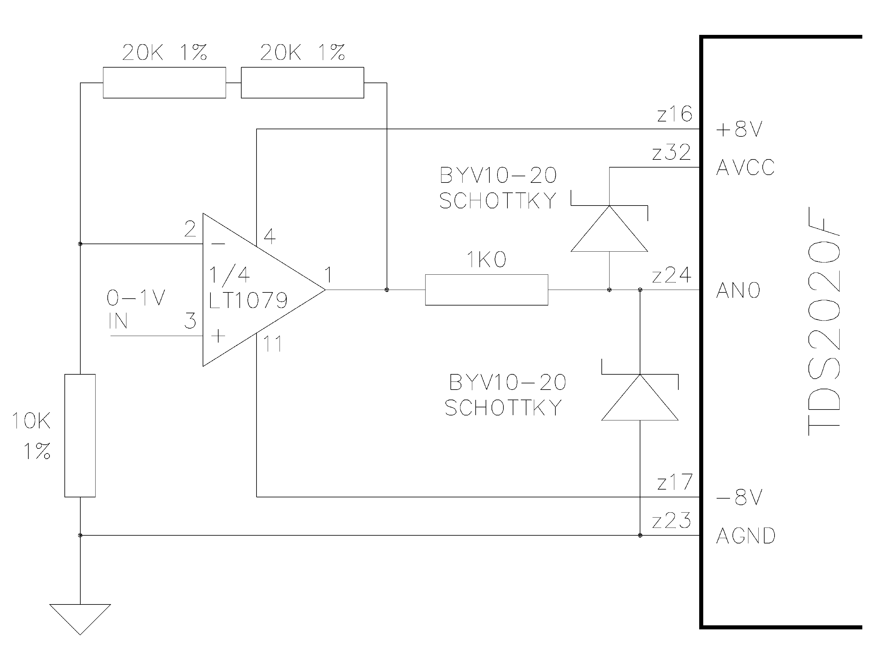
A to D input amplifier suggestion Input voltages must not exceed 0.3V beyond the AGND to AVCC range. If necessary put Schottky clipping diodes from the inputs to each reference rail. Signal conditioning circuits to amplify transducer signals to the 0-5V range could be conveniently made on a sub-board plugging into the top of the TDS2020F. You will find that all signals and power supplies needed are grouped to one end of the computer so that the sub-board need not be the full 100mm width. The diagram shows a suitable amplifier, with protection for the A to D inputs of the microprocessor. You can access different modes of the A to D converter directly, see Section 15 of the Hardware Manual for details. For example the converter can be made free running so that it scans 4 channels. In this way the converted value is available at any time from register locations. Down to 13�s conversion time is possible. For greater resolution attach external ICs. Serial chips have the advantage that they can be kept away from fast digital noise. See 12-bit 8-CHANNEL A TO D CONVERTER, page 298. This uses the MAX186 serial A to D device. For greater resolution and both serial and fast parallel connection, see 16-bit 4-CHANNEL A TO D CONVERTER, page 298. |
 |
|